
| Power Electronics
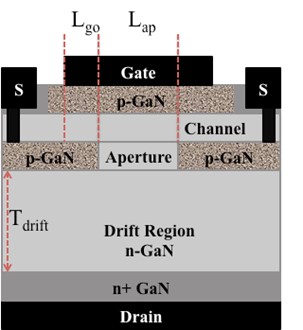
In collaboration with UCSB, this project aims to develop new vertical GaN transistors that will significantly enhance the performance and reduce the cost of high power electronics. Bulk GaN devices delivering 1.2kV switches form the core of our research. |
 |
| Fabrication and optimization of lateral AlGaN/GaN MISHEMT with field-plates structure. High breakdown voltage up to 1kV. | 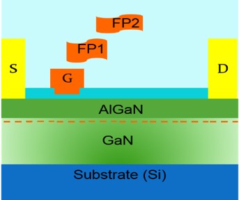 |
|
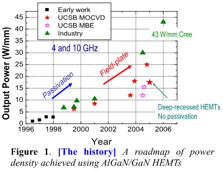
High Frequency Electronics It is critical that the Power Density and Power Added Efficiency (PAE) of RF RADAR amplifiers be maximized to reduce chip size and thermal cooling requirements. This enables new RADAR amplifier Classes such as switched mode amplifiers, reduces electrical and thermal system complexity and cost while simultaneously simplifying deployment. Vertical GaN-based transistors uniquely harness the high breakdown field of GaN because the electric field distribution is uniform, easily designed and contained in the bulk of the device compared to peaked surface/interface electric field distribution in lateral devices. Coupled with the reduced dispersion at high voltage they provide the desired high power density and PAE not possible with current technology. |
|
| Terahertz Electronics
The performance gap preventing transistor operation at or near the terahertz regime makes the development of ultra-broadband wireless communication, advanced imaging and radar, electronic THz spectroscopy and THz digital computation, all critical components to enhance war-fighter capabilities, increasingly difficult. To overcome this performance gap, we are looking into novel approaches tailoring E-k space to energize an electron beyond what is possible by scattering dominated transport. |
|
| High Temperature Electronics
Developing stable and low-resistivity ohmic contacts to GaN for high temperature InGaN solar cell operating above 450 ºC. The high temperature InGaN solar cell will be attached to concentrated solar power to form a hybrid solar converter which could convert solar energy at higher efficiency and also provide dispatchable energy. |
 |
|
Diamond Electronics Diamond is the ultimate material for power electronics. Diamond’s wide band-gap, high predicted mobility and excellent thermal properties makes it an excellent candidate for future power devices. The progress with respect to diamond electronics has been impeded mainly due to the difficulty in growing homoepitaxial diamond (especially n-type) and the availability of single crystal bulk diamond substrates. The low work function of n-type diamond (0.9 eV) makes it difficult to form ohmic contacts.During the course of the project we have developed ohmic contacts to n-type diamond enabled by development of a novel growth scheme in Dr. Robert Nemanich’s group at ASU where Phosphorus doped n-type films with high doping can be grown epitaxially. The final goal of the project is to develop a 1.2 kV diamond based Bipolar Junction Transistor and a 5kV diode. Moreover, Surface conduction by a 2D-hole gas formed through hydrogen termination, a property unique to diamond, can be utilized to make lateral FETs that can operate as high as 120 GHz. Our research also involves pushing beyond these limits of frequency and power in lateral diamond FETs by improving different parameters that operate the lateral FETs. Selected Publication :
|
|
N-Polar Design, simulation, fabrication and testing of new N-Polar GaN-based unit cells for highly efficient integrated power conversion. The majority of GaN devices are produced with materials grown with Ga-polarity in the c-plane. Accordingly, the majority of current GaN device designs cannot achieve functions that are achievable by material properties that require material grown with N-polarity. Consequently, considering such limitations of previous technological approaches, it would be desirable to have a system and method for a III-nitride vertical transistor with the above-mentioned functionality. |
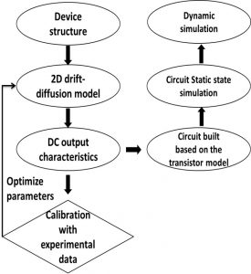
| Modeling and Simulation
In our group we also carry out 2D TCAD device simulation using tools such as SILVACO (ATLAS). Extensive 2D simulations of vertical as well as horizontal devices have been done. These simulations enabled device behavior predictions and thorough analysis of device I-V and C-V characteristics. Moreover, compact modeling and circuit simulation of the later as well as the vertical devices fabricated in the group is also being done. Our group focus on physics-based compact models as they are known to be the most robust and reliable compact models. In our group we use physics-based compact models for lateral HEMTs that are previously developed by some of the group members. Compact modeling of the vertical devices is significant part of our current research focus. This enables us to evaluate and further study the performance of the devices in various sub-circuits that have got applications ranging from DC to RF. |
 |